


Memory is one of the most fascinating storylines of the current AI build. It used to be a perennially cyclical business. But data center demand has changed everything. There is a very strong argument to be made it is structurally in demand.
Cynics still argue that memory is, at the end of the day, a “commodity” and once the capacity picks up, their pricing will revert back to normalcy if not cratering. A couple of years back, DRAM and NAND diverged sharply.
Even the hardest of cynics have more or less agreed that with HBM (DRAM), the technology moat means the current status will remain longer, which leaves NAND at a tough spot.
SK Hynix and SanDisk first announced a joint agreement on HBF standardization. Google and Tenstorrent joined at the February formation and finally META joined at the August spec release. Google and META participation brings major hyperscaler validation to the OCP workstream. With the launch of HBF, is NAND also getting structural leeway?
To read my full disclaimer please click here
Before all that, let’s look at some basics
First, the basics
There are three kinds of memory differing mainly in two ways: how quickly the processor can reach them and cost per gigabyte. They are inversely correlated. The faster the reach, the costlier the memory.
SRAM: Sits on the processor. Fastest of the three and the most expensive. It is used for caching because it has constraints that rule it out elsewhere. SRAM faces strict physical die-area constraints. Large cell size prevents SRAM from scaling beyond a few hundred megabytes.
DRAM: the working memory. Cheaper than SRAM but more expensive than NAND. Dynamic and enables swift read and write. It is volatile, meaning it loses everything when disconnected from power.
NAND: the storage memory. Cheapest of all. It’s in SSDs and can hold a far larger volume of data. It is non-volatile but has roughly 1000x higher access latency (reads slower) than DRAM. It also faces endurance issues, limiting read/write cycles.
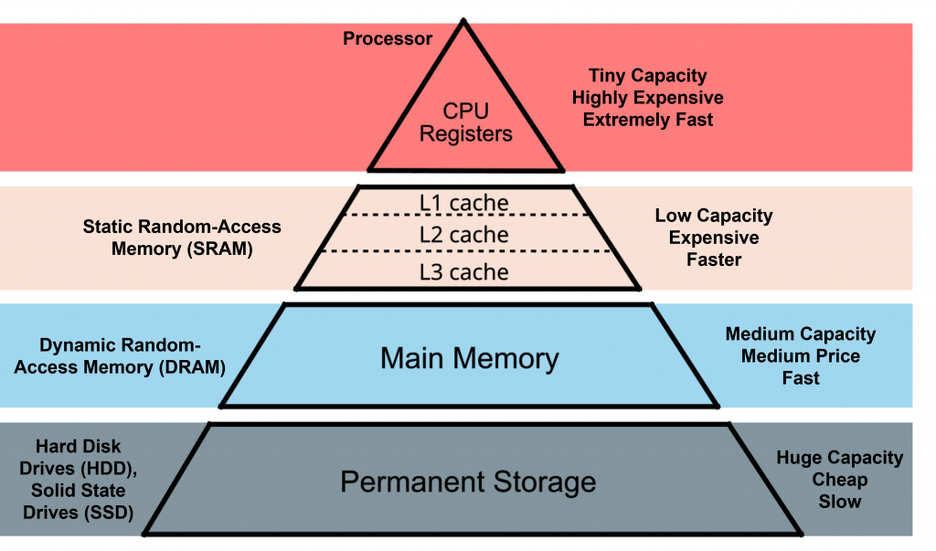
Traditionally, the roles were clearly defined. You use NAND for storing data (cold storage), use RAM for on-the-go processing. However, modern workloads, especially AI inference, high-speed networking, and massive parallel compute have pushed the boundaries, blurring the lines.
One of the biggest challenges that traditional memories weren’t able to solve was the “Memory wall”. Compute speeds have outgrown the bandwidth that DRAM can supply. It is important to understand that GPUs (and compute in general) are very valuable. The limited memory bandwidth increased GPU idle time.
SRAM cannot be used because it does not have the capacity, occupies a large area for the same memory, draws significantly more power and is very expensive. NAND cannot be used because of latency, thermal limitations and endurance limits.
That’s where HBM comes in.
Before going any further into that, I think spending couple of minutes on the below video from the SanDisk investor day would make a lot of concepts we will be discussing easy to follow. Do check it out.
HBM - High Bandwidth Memory
Why did the “memory wall” problem exist: Data starvation. Modern GPUs are capable of handling thousands of parallel threads. They need massive volumes of data fed into them simultaneously. The core problem was bandwidth.
To overcome this challenge, DRAM makers took a very interesting approach:
Stack multiple DRAM dies on top of each other to increase the bandwidth of data flow (and capacity).
Bring it as close as possible to GPUs to reduce time wasted in transmission.
Latency is still there but increased bandwidth reduces GPU idle time significantly.
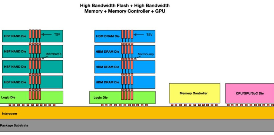
HBM is the repackaging of standard DRAM. It uses 3D vertical stacking via TSVs (Through-Silicon Vias) and stacks multiple DRAM dies on top of each other on a base die. HBM stacks are then placed on an interposer right next to the processor rather than a PCB bus. By doing this, speeds went from ~50 GB/s to multi TB/s.
HBM’s competitive moat that even the cynics aren’t able to fully dispute comes from:
Base HBM die: Until HBM3E, the base die was standardized. Customizations were minimal. GPU vendors bought standard JEDEC-spec stacks. That changes with HBM4. Each base die, on top of which DRAM dies are stacked, is unique and customized for each customer.
TSV yield: Stacking DRAMs itself is a very complex process with very low yield. A failure in a single TSV can waste the entire HBM stack. Considering each stack has 8-12 DRAM layers, it creates a huge manufacturing complexity that is difficult for a new entrant to overcome.
High switching cost: HBM stacks sit right next to GPUs mounted on interposers. So replacing them isn’t as easy as a component swap. In future, switching becomes even harder because of the custom base HBM die. Each new vendor would have to go through a rigorous, complex qualification cycle that demands investment.
The combination of this moat and higher demand of DRAM (one bit of HBM needs a lot more DRAM wafers than commodity DRAM) gave the DRAM makers longer leeway when it comes to valuations and demand. Even the most cynical critic acknowledged that DRAM players will be in demand longer than their commoditized past.
If you are a critical person, the natural question that should arise is why can’t someone stack NAND and solve the same problem.
That’s where HBF comes in.
HBF - High Bandwidth Flash
Before that, it’s important to understand the limitations NAND has:
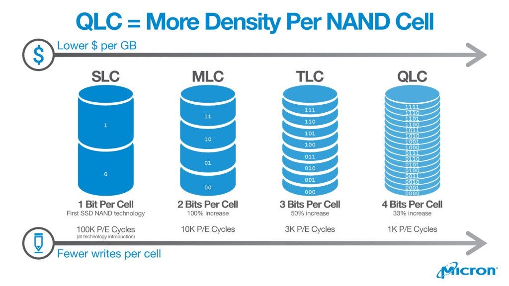
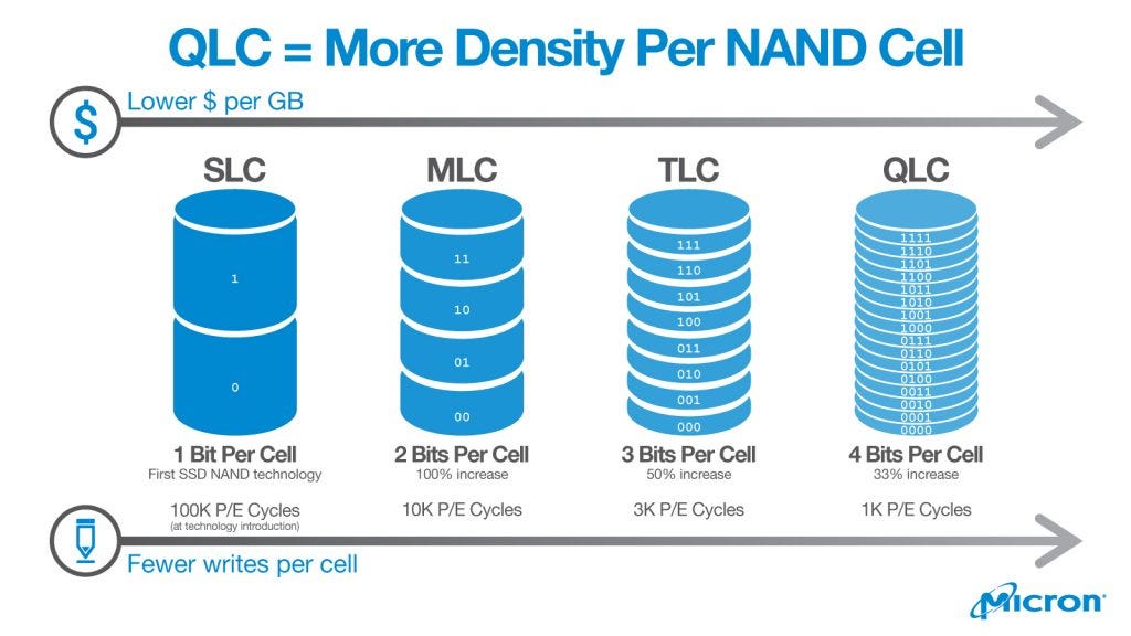
Writing often wears down flash memory: Writing means forcing charge through the bits. Slow degradation is unavoidable for every charging cycle. The higher the bits per cell, the higher the degradation rate. So the higher the capacity, the fewer the write cycles.
Reading from NAND flash memory is slow: Flash stores data as trapped charge and reading it means measuring how much charge is there. It comes in various configurations of bits per cell. Lower bits mean faster reading, higher bits mean larger storage. Due to its application, the industry always chose TLC/QLC which enables higher capacity at the expense of read/write latency and endurance.
Latency in data retrieval: The biggest challenge of NAND flash memory. It was designed to store data. It has a narrow interface and reads sequentially.
Flash memory has poor thermal properties: As the heat increases, the charge stored can escape (leaks) meaning the higher the temperature, the lower the retention. If one mounts charge-trap NAND on an interposer directly adjacent to a high-TDP GPU (800W+), it will result in rapid charge leakage and data loss. Worse yet, if thermal stress corrupts the flash die, you are essentially wasting an extremely expensive chipset.
“HBF is a new concept in memory that applies TSV technology—similar to HBM—to achieve both the large capacity of traditional storage and high bandwidth comparable to DRAM. It holds significant potential to establish itself as a new memory tier between ultra-high-speed HBM and high-capacity SSDs.”
- SK Hynix Vice President Lim Eui-cheol
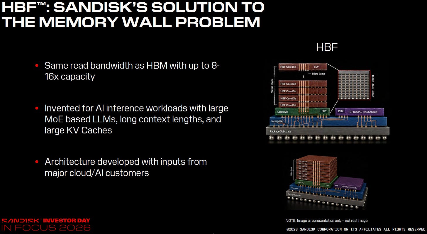
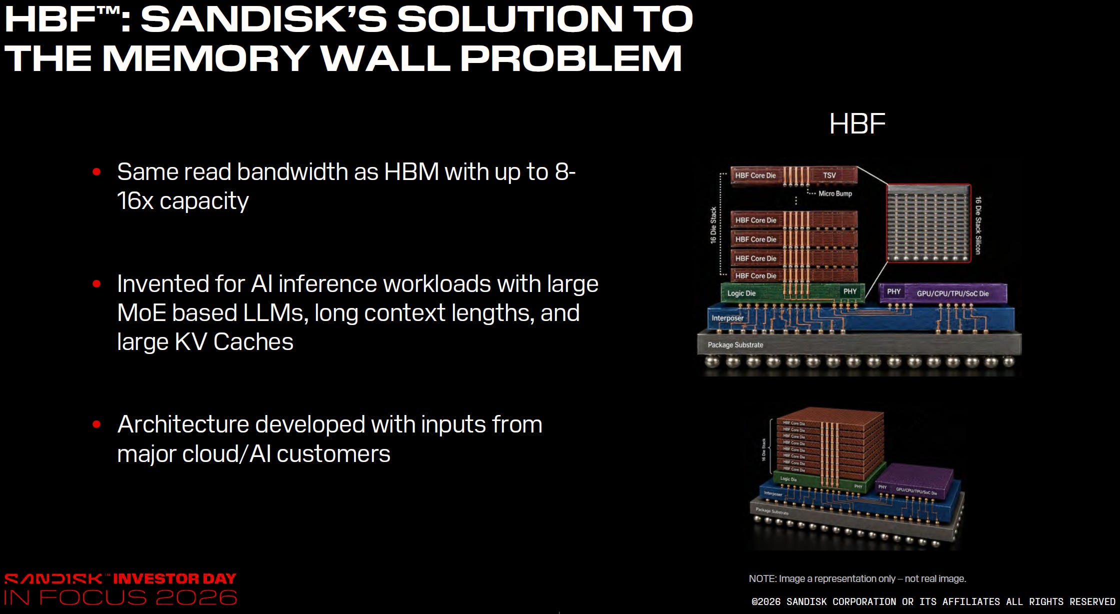
HBF is constructed to overcome some of these challenges. It’s basically the same as HBM, just that instead of stacking DRAMs on a base die via TSVs, HBF stacks NAND on a base die.
The spec for HBF was published in early August: up to 512GB; eight- and sixteen-high; three bandwidth grades from 0.4 to 3.0 TB/s; over UCIe, plus host interface, electrical, packaging and reliability guidance.
What does and doesn’t HBF solve?
Now that we understand the limitations and what HBF is on a superficial level, let’s deep-dive into its architectural choices and how they attack the limitations
pSLC over TLC/QLC/MLC:
Instead of running on multicell architectures (TLC/QLC/MLC), HBF configures its dies on single-bit pseudo SLC (pSLC).
What it solves: Drastically accelerates cell-sensing time. As it measures charge in a single cell (reading) instead of multiple, latency is reduced.
What it doesn’t solve: The trade-off for choosing pSLC is that the memory density reduces significantly. Raw storage capacity per stack is reduced by 3-4x. Reduces the cost/GB advantage that NAND has over DRAM.
Source: SanDisk presentation for investor day held on Aug’26
Restricting writing workload
HBF is architected explicitly as a static read-only repository for model weights, rather than general-purpose working RAM.
What it solves: Limiting the writing frequency on the HBF eliminates write wear and oxide layer degradation. Model weights are written once during initialization and read millions of times. This bypasses the endurance limits as reading doesn’t force current into the flash memory.
What it doesn’t solve: It still cannot replace HBM fully as it cannot support KV cache (or any function requiring dynamic read/write). It can be a good model storage vehicle during inference but for training applications, the architecture is simply not viable.
TSV Vertical Stacking via Wide UCIe Interconnects
HBF replaces narrow sequential channels with wide, multi-channel host interfaces. Stacks up to 16 NAND dies vertically via Through-Silicon Vias (TSVs) linked to a custom logic base die and a high-speed UCIe chiplet interface. Picture this: to carry tonnes of goods, rather than making the truck bigger, HBF enables 1,000 trucks to carry the load. Load being the data in this analogy.
What it solves: By enabling thousands of reads in parallel, HBF suddenly unlocks massive bandwidth. It enables a massive multi-terabyte streaming pipeline (up to 3.0 TB/s per stack), feeding GPUs at scale. It offers HBM-level bandwidth at a cheaper price and higher storage capacity.
What it doesn’t solve: HBF “can” meet the bandwidth of HBM. But it still cannot overcome the fundamental latency that an individual NAND unit (~10-25 microseconds) has versus a DRAM unit (~15 nanoseconds). An HBF cell read takes roughly 700-1,700 times longer than a DRAM read. There are some predictability challenges that need to be architected around if both HBF and HBM are used.
Thermal & manufacturing limitations
Beyond all this, HBF also hasn’t categorically proven that it can withstand the thermal exposure it is bound to be under. Even if they are somehow packaged away from the GPU, the read frequency will increase the temperature, which could result in bricking the entire chipset.
“What determines overall efficiency is where each memory tier — HBM, DRAM, NAND (HBF), and SSD — is positioned and how it is connected to minimize data movement.”
- Kim Chun-sung, SK Hynix Executive VP and Head of Solution Development
HBF, a competitor of HBM?
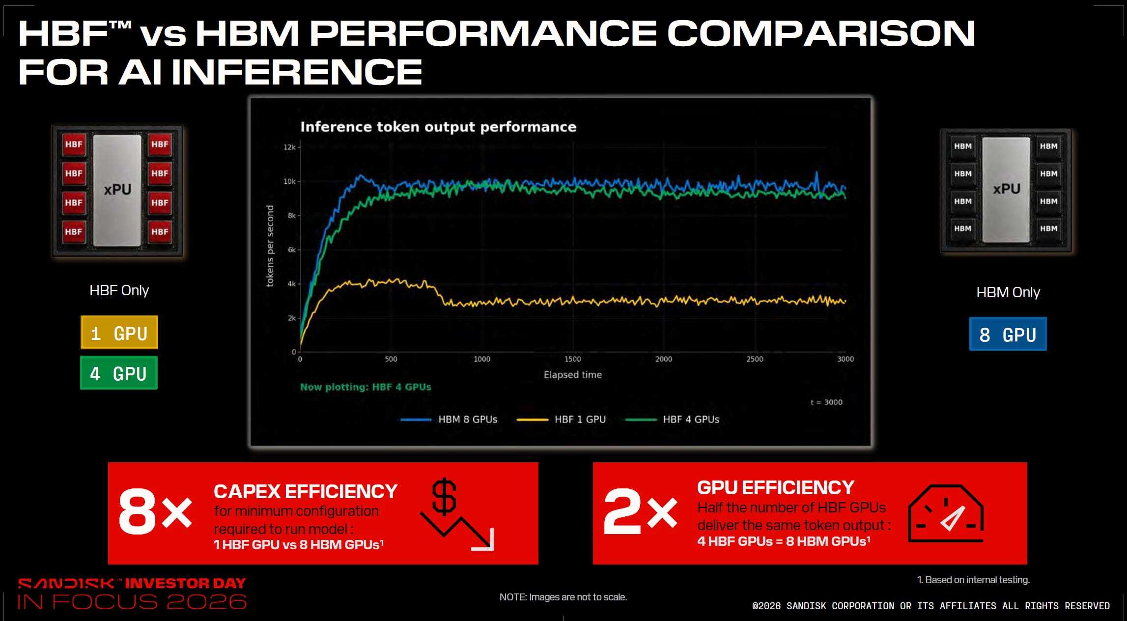
SanDisk certainly thinks so and at their investor day even shared that using HBF requires fewer GPUs compared to HBM and their inference token output was better despite using half the GPUs.
The caveat though is that this works only until a point because of higher initial latency, worse performance under heavy multi-user loads, and flash wear limits. All this means HBF is more suited as a complementary solution than a replacement solution.
There has been early pushback at the comparison. The HBM baseline used was two generations old. The weights were assumed to be BF16 when most of the inference has already moved to FP8 or lower. Write endurance was never mentioned at all. Despite all pushback, the directional application is still intact.
HBF can still meaningfully reduce the dependence on HBM by complementing it in inference creating a two-tier memory architecture.
Tier 1 (Hot memory): Reserved for dynamic, high-frequency read/write operations like KV-caches, activation scratchpads, and volatile execution state. It requires nanosecond latency and very high write endurance.
Tier 2 (Warm memory): Reserved for static, read-only LLMs and their weights. Weights are written once during context load and read millions of times during inference.
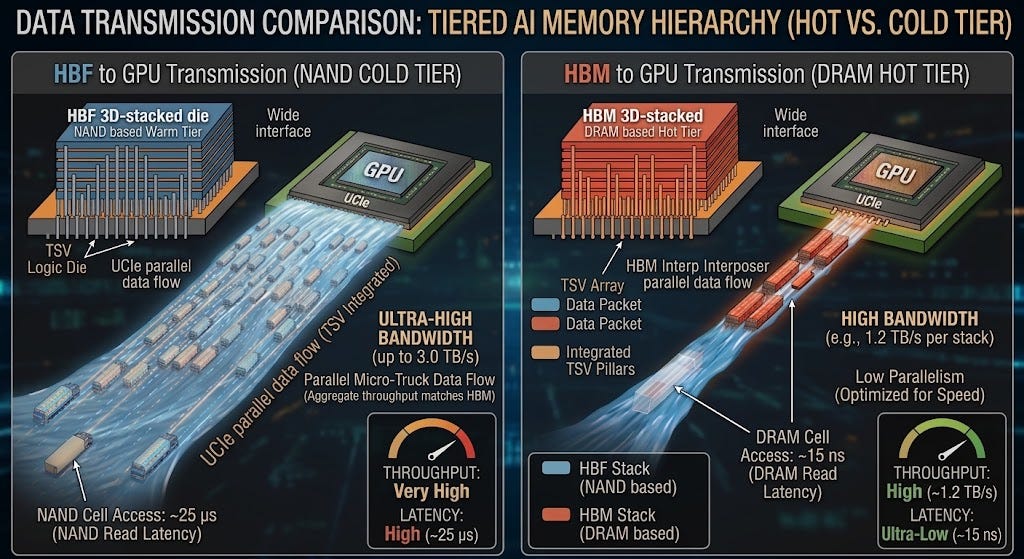
By pairing HBM and HBF via UCIe on an interposer or substrate, you can scale model parameter capacity by 8–16x at a fraction of the cost per gigabyte. One can preserve expensive HBM capacity strictly for latency-critical KV-cache expansion and use HBF capacity for model storage.
Alternative solutions
HBM demand has been such an acute problem that there are multiple stakeholders who are already working to solve it. Each approach has its own solution and its own problem. Some notable attempts ongoing are:
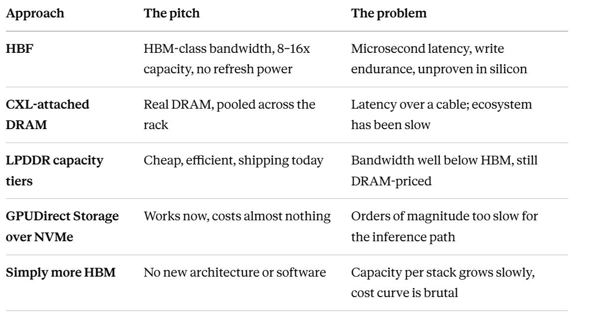
HBF must now compete with all of these approaches and prove itself as a cost-effective, viable solution with a relative ease of implementation to avoid scaling challenges.
There is one underrated issue that could crop up if HBF is indeed paired with HBM. There is an inherent need to orchestrate the whole data movement between HBF, HBM and GPUs. This can be done at a software layer but the downside is that it creates another challenge in adoption.
Compute vendors like NVIDIA or Broadcom would have to accept the added complexity in the framework making their commitment one of the key milestones for the technology.
"AI inference is creating a new set of memory requirements, and HBF technology is designed to meet that moment. This specification helps give system designers a practical path to bring high-capacity, high-bandwidth memory closer to compute... It is an important milestone for the HBF ecosystem and for the next generation of AI systems built to improve token economics at scale."
- Alper Ilkbahar, CTO, SanDisk
What does all this mean for NAND demand?
Well, let’s look at some facts. What does the market say about NAND demand?
One of the clearer forecasts came from Morgan Stanley in early July, before the bloodbath.
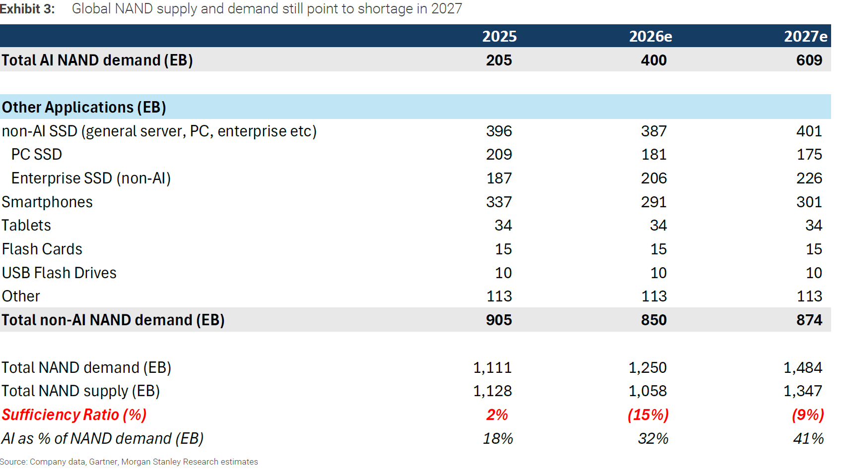
AI demand for NAND is expected to triple from 2025 to 2027. While demand is hitting unprecedented levels, simultaneously the inventory levels at NAND suppliers are also at a multi-year low. Inventory situation improving at server players & major model houses though.
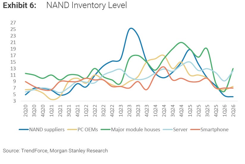
Though the report is ~2 months old, the underlying situation is very much intact. In fact this was also confirmed by SanDisk themselves through their internal estimates.
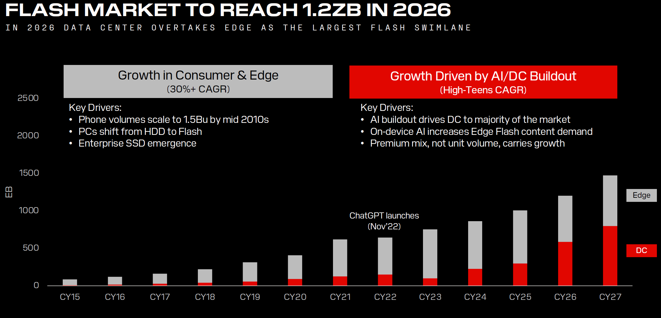
HBF can be a meaningful tailwind or fuel to the fire for the current situation. A commodity BiCS8 die, which SanDisk & Kioxia ship in volume today, carries roughly a terabit in three-bit mode. HBF at its current spec has 256 gigabits on each die. Configuring 3D NAND into single-bit pseudo-SLC (pSLC) reduces raw bit density per die by ~3–4x.
That means every gigabyte of HBF consumes three to four times the wafer area of a gigabyte of ordinary flash. Wafer capacity is what sets the NAND cycle. So HBF tightens supply three to four times faster than its gigabyte volumes would suggest. Even modest adoption will tighten an industry already running a deficit.
The bottom line is that whether HBF flies or not, the demand for NAND is unprecedented. HBF acts as a tailwind by creating a structural moat against commoditization and could stave off a sudden supply glut from China, if and when one arrives. If HBF doesn’t go through, the knife of cyclicality will keep hanging over the head of NAND.
Key risks
There are some other non-architectural risks though:
Complex manufacturing: Stacking 16 dies of NAND on top of a base die is a manufacturing nightmare. It takes years of process mastery and know-how that cannot just be bought. SK Hynix’s experience with HBM might be a crucial element driving / slowing down the maturity.
Deteriorating Yield: Assuming a 98% yield in a traditional NAND, stacking 16 NAND dies on top means the overall yield for HBF tumbles down to 72.38%. HBM manufacturers underwent the same problem but now have overcome it. HBF players will need a similar maturity curve before industry-wide adoption.
Long term vs Short term: NAND is in the tightest shortage it has ever seen. Established players must be willing to sell high-value, long-term-oriented HBF over high-profit, short-term, demand-driven commodity NAND. Might not be an easy sell to the shareholders.
TSV Capacity: HBM and HBF both compete for the same TSV capacity, the same hybrid bonders, the same test slots, the same interposer and substrate area inside a package. HBM clearly is at a higher maturity curve than where HBF is right now. The risk is whether the development and ramp up of both HBM and HBF can happen simultaneously.
Worth watching:
NVIDIA joins the consortium or puts HBF on a public roadmap. It would take HBF from a niche consortium project to an industry tier.
Strong hyperscaler commitment. Google and META haven’t disclosed anything on deployment. Any sort of commitment will be a tailwind.
Product performance: It’s still very much an initiative right now with real samples months away. When released, performance and stability will be the true test of the long-term viability of the product.
Retention and error rates at operating temperature come in strong on real silicon. Claims are not measurements.
Conclusion
HBF is a good (very) early stage engineering product aimed at a real problem crippling the industry and the AI build. But not all products / engineering solutions work out. HBF, at best, is complementary to HBM rather than a replacement. At the end of the day HBF is made of NAND, which has fundamental engineering limitations if it aims to replace HBM.
Having said that, it is equally important to understand what HBF brings to the table: A great complementary product to reduce HBM dependence. When paired with HBM it offers significant cost benefits.
It is not without its risks though and for all the hype, the product isn’t even expected to be commercially available in the next 24 months. Add to that: how motivated would established players like Kioxia and SanDisk really be to push HBF at the expense of selling high margin commodity NAND which is facing historic demand?
These are same questions HBM vendors also faced. They ended up allocating capacity toward HBM product lines, supply of less profitable products tightened until pricing improved. NAND players likely follow the same path only that the NAND prices are already at all time highs.
We do have a small favor to ask…
If you got value out of this article, we would really appreciate if you can spread the word amongst your friends, family or social media. We see it as a huge token of recognition from you. Thanks a lot for your time.
Any questions about this post or other things regarding stock market? Questions about some of our holdings? Let us hear them in the comments!
Please do restack, share and comment as a show of your approval (or disapproval) of the content