

Know your Substrate - Decoding Front-End Wafers
Mapping the materials science, manufacturing layers, and critical pricing power bottlenecks that separate front-end wafers from back-end carriers. Long-term investor's guide to front-end wafer.

During the early onset of semiconductor craze in 2020 (yes there was one before now), one of the most confusing thing for me what does “wafer” even mean. I often (stupidly) assumed that the PCBs were the “wafers”. It took the first chip shortage hit my work in a reputed automotive company, for me to actually delve deeper into the topic.
It was very challenging and confusing, as expected, to understand various terminologies like substrates, wafers, ABF, silica sand et al. It took a lot of time for me to declutter all this in pre GPT era.
The aim of the article is to make this journey easier for you by walking through various layers of manufacturing and list down crucial names across the value chain. Let’s begin
To read my full disclaimer please click here
Before everything, this video from AMAT 0.00%↑ is a very good place to begin your journey.
Why the wafer?
In the pre bottleneck era, wafers were just the silent, studious set of companies who just silently went about their job with little attention. The importance were always understood and respected. Transistors weren’t grown out of trees, rather they were literally grown on polished disc of crystals aka wafer.
Properties of that disc set the ceiling for everything above it: how fast the chip can switch, how much heat and voltage it survives, whether it can carry light instead of electricity at all. The material decides what is possible, and only then does the clever design get to do its work.
Wafer layer is one of the quietest and most durable oligopolies in all of technology. Growing a defect-free crystal disc, atom by atom, at industrial scale, is one of the genuinely hard manufacturing problems left on earth. It requires decades of process craft that is difficult to buy off a shelf.
That kind of moat is exactly the sort that survives a downturn. It is a place worth understanding before investing. They are essentially the foundation of semiconductors.
What "substrate" means?
Substrate is the foundational base material upon which integrated circuits and transistors are fabricated. It provides crucial physical support, thermal management, and electrical connectivity for microelectronic devices.
“Wafer” is the physical form factor, while “Substrate” is the functional role.
The industry uses the word "substrate" for two completely different things, and confusing them is the fastest way to get lost, so let me draw the line before we start.
Front end substrates: Wafer in itself on top of which chips are made. The polished discs of single-crystal material upon which transistors are physically built inside the fabrication plant (fab). This material defines the physical and electrical ceiling of the completed chip.
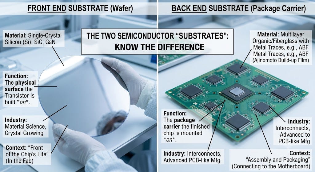
Back end substrates: High-density organic or inorganic carriers upon which finished silicon chips are mounted during assembly to interface with a printed circuit board (PCB). This is an interconnect industry structurally closer to advanced electronics manufacturing.
This post covers primarily front end substrates. I have laid this out as a chain, the same way I did the nuclear ecosystem, for easier breakdown.

The first section walks the process: how a fistful of purified sand becomes a finished wafer, step by step, from raw silicon through to the epitaxial coating, with the companies that own each step.
The second section walks the variations: the engineered and exotic substrates, SOI, silicon carbide, gallium nitride, indium phosphide and a few honorable mentions, that do the jobs plain silicon cannot, and where the tightest monopolies in the whole industry happen to live.
The intention is not to teach you materials science. It is to show you where the bottlenecks and the pricing power sit.
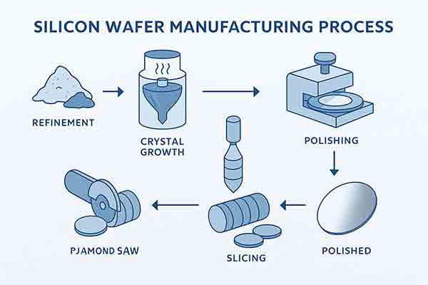
Section I: The Base Silicon Process
Silicon, passes through four stages before it is ready to become a wafer chip. For every material, there will be “names to watch” and “nature of business”
Stage 1: Polysilicon Purification
It begins with silicon refined to a purity that is genuinely difficult to picture. The electronic grade that becomes a chip is eleven nines pure, 99.999999999%, meaning one stray foreign atom for every hundred billion silicon atoms.
This is a different animal from the solar-grade polysilicon. There is abundance there, and some producers make both, but the gap between the two grades is huge, which is precisely why the electronic grade carries such pricing power. It is the feedstock for every silicon wafer downstream.
Nature of business: Defensive and unglamorous. In 2025 with a Section 232 investigation into polysilicon imports, US reemphasized its importance.
Names to watch: ~75% of market is held by 2 companies: Wacker Chemie (WCH.DE) and privately held Hemlock Semiconductor (majority Corning). Japan’s Tokuyama (4043.T) and Mitsubishi Materials (5711.T) are other big names. Leader is Wacker who also have a broader chemicals and solar business under same roof.
Stage 2: Single-Crystal Ingot Growth
The polysilicon from Stage 1 is pure, but it is in the wrong physical form. The clue is in the name: polysilicon is a jumble of many small crystals fused together. A chip cannot be built on a jumble. It needs one continuous, flawless crystal with a single lattice orientation running end to end. Stage 2 is where that transformation happens through a method called Czochralski pulling.
High-purity polycrystalline silicon is melted in a quartz crucible [A] inside a Czochralski puller under a controlled argon atmosphere, heated by a resistance element. Once the melt stabilizes near silicon's melting point of ~1,412°C, a rotating single-crystal seed is dipped into it [B]. A slight temperature drop starts silicon crystallizing onto the seed [C].
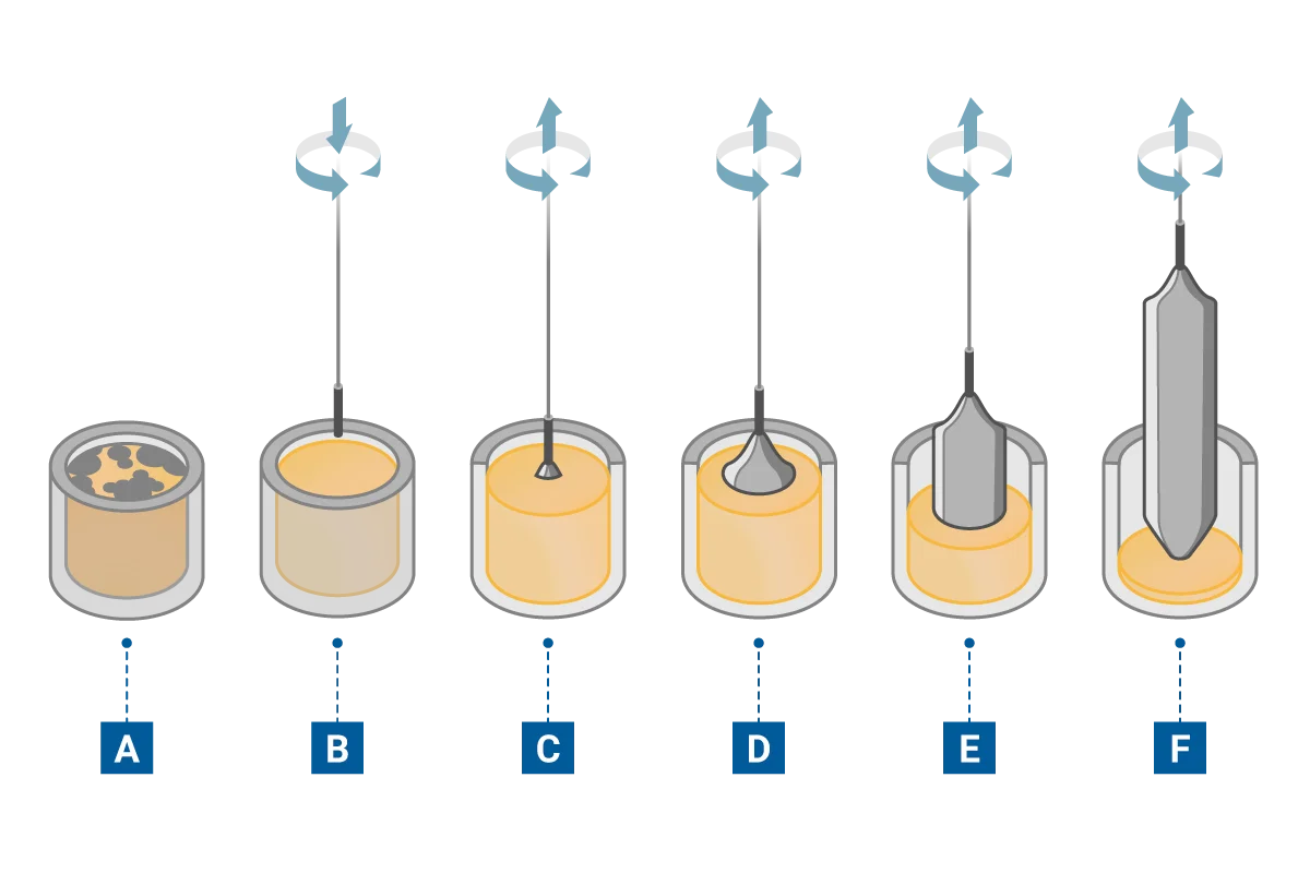
As the seed is drawn slowly upward a cylindrical single-crystal ingot forms beneath it [D]. Controlling the pull speed, the crystal and crucible rotation, and the temperature gradient holds the ingot at a constant diameter while it inherits the seed’s lattice orientation [E–F]. Germanium uses the same method with a graphite crucible instead of quartz and lower temperatures, matched to its ~938°C melting point.
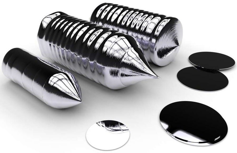
Nature of business: Process craft, and the hardest, least visible part of the moat in the whole chain. A single misplaced atom or trapped impurity turns every wafer sliced from that section into scrap. This is the reason “silicon-wafer startup” aren’t common: no amount of capital cuts the decades of furnace know-how it takes.
Names to watch: No standalone players. Growing the crystal and slicing it are a single integrated craft, folded inside the wafer majors in Stage 3.
Stage 3: Slicing, Etching, and Polishing (Prime Wafers)
Then ingots are then sliced, processed and polished to form Prime silicon wafers. Almost entire chip industry runs on the base of this chips. It comes mainly in 2 diameter variations: 200mm & 300mm.
The 300mm wafer carries the advanced money: the logic in CPUs, GPUs and AI accelerators, and the DRAM, NAND and high-bandwidth memory those systems need. That is the segment the AI build is pulling hardest.
The older 200mm wafer still runs an enormous business underneath, carrying the power-management, analog, microcontroller, image-sensor and display-driver chips that fill every car, phone and appliance.
Nature of business: Oligopolistic in nature with 5 players dominating it. MOAT is deep owing to high entry barrier & decades of process know-how and customer relationship. Qualifying a new wafer supplier can take years. It is cyclical.
Names to watch: Shin-Etsu Chemical (4063.T) and SUMCO (3436.T) hold roughly half the 300mm market between them, with GlobalWafers (6488.TWO), Siltronic (WAF.DE) and Korea's SK Siltron (inside SK Group, not separately listed) making up the rest (industry estimates, flagged). Leader: Shin-Etsu.
Stage 4: Epitaxial Coating (Epi Wafers)
Last step: A layer of coating is grown on top of the prime polished silicon wafer. It carries most of the electrical performance while the base wafer offers mechanical support. Unlike steps 1 - 3, this is done not on all chips because epitaxy is an extra, expensive step, and a plain polished wafer is already good enough for many chips.
At the end of stage 2, causes some impurity / defects stay on the wafer. For many applications like memory or standard logic, this imperfection is acceptable. Epi skin are essential when the device physics demands something just prime silicon wafer cannot give: a layer far cleaner and more precisely doped.
Applications like image sensor in phone, power devices, CMOS require this. Epitaxy is also the bridge into the variations below, because growing gallium nitride on a silicon wafer is itself an epitaxy problem.
Nature of business: Value-add layer sold at a premium over bare polished discs, and often captured captively inside the device makers. The one listed pure-play behaves like the small, cyclical, single-technology bet it is.
Names to watch: IQE (IQE.L) is the listed specialist, growing the compound-semiconductor films that go into smartphone RF front-ends and photonics. The Stage-3 majors also sell epi wafers at a premium. Leader: fragmented.
Section II: Material Variations & Structural Moats
When industry applications outgrows standard silicon, specialized compound materials are added to the base chips. This is where hyper-concentrated monopolies emerge. Each variation will have “Application” and “Problems it solves” section in addition to give context
SOI, silicon-on-insulator: the French near-monopoly
Problem it solves: Ordinary silicon is slightly conductive, so at radio frequencies the signal leaks down into the bulk wafer, wasting power and adding noise. It also enables a phenomenon called “parasitic capacitance” (check glossary in the bottom). Plain silicon is a leaky, sluggish foundation for a high-frequency or ultra-low-power chip.
Parasitic capacitance = an unwanted capacitor that forms between a transistor & the conductive silicon wafer beneath it. Every switch has to charge/drain it first, which wastes time and power.
SOI fixes these problems with a clever sandwich. It kills the leakage, and by pushing the transistor away from the substrate, shrinks the parasitic capacitor to almost nothing. There are two ways to build it:
Bonding (the dominant method): oxidise one wafer's surface into glass, bond it face-down onto a handle wafer so the glass is trapped between them, then thin the top wafer to a sliver of silicon.
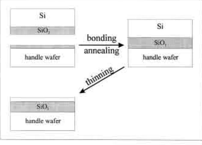
Source: University Wafer. Oxygen implantation (SIMOX): fire oxygen ions deep into a single wafer and anneal, so the buried glass forms in place.
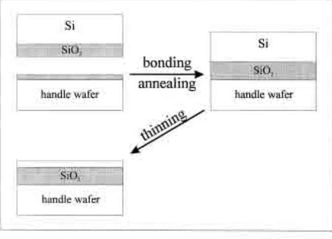
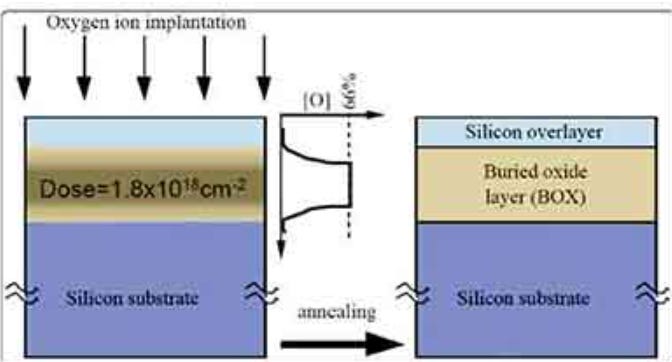
Either way, the same stack results, top to bottom: thin working silicon, buried glass, thick support silicon. The result is a chip that switches faster while sipping far less power. The same buried insulator also confines light, which is why it matters for photonics.
Application: SOI are used when higher switching speeds, better power efficiency & Monolithic integrations are needed. Two main applications for SOI Wafer: RF SOI & Silicon photonics.
RF-SOI: used in high-frequency wireless communications to build front-end modules. It powers components like antenna tuners, RF switches, and power amplifiers. Are used in smartphones, automotive, wearables etc
Silicon Photonics: Silicon-on-Insulator (SOI) technology is the core foundation of silicon photonics. It traps infrared light like tiny fiber optic cables right on a chip, combining high-speed electronics and optical logic at the speed of light.
Nature of business: Near-monopoly of SOITEC built on a proprietary process called Smart Cut, Soitec's bonding & splitting method that sits behind nearly every SOI wafer made. Others make SOI too (Shin-Etsu, GlobalWafers, SUMCO), but mostly under a Smart Cut license and in photonics-grade SOI it is the only qualified volume supplier. Licensed IP plus sole-supplier status: Rare double moat
Name(s): Soitec (SOI.PA) estimated to make the large majority of the world's SOI wafers. Leader: Soitec, decisively. Shin-Etsu (4063.T) (the main Smart Cut licensee), GlobalWafers (6488.TWO) and SUMCO (3436.T) make mostly general-purpose SOI and sit well behind
Silicon carbide, SiC: the battlefield
Problem it solves: silicon breaks down under high voltage and gives up at high temperature. To handle serious voltage a silicon power device has to be built thick, and thick silicon conducts poorly, which wastes energy as heat every time it switches. That is dead weight in an EV, where every watt lost is range lost.
Silicon carbide handles high voltage and high temperature far better than silicon, tolerating roughly ten times the breakdown field and switching with far lower losses.
Application: EV powertrain. Used in traction inverter & onboard charger, where switching power more efficiently translates into range. Beyond cars, it also serves DC fast-charging stations, solar/wind inverters, industrial power supplies, rail and grid electronics.
However, a critical second structural growth curve has emerged in AI Datacenters. Specifically its use as thermal interposers in next-generation AI platforms (like NVIDIA's Rubin) to manage extreme GPU heat loads emerging .
Nature of business: Most contested substrate on the board, and the cautionary tale of this whole piece. Chinese share climbed from around a tenth in 2021 to near forty percent by 2024, collapsing substrate prices by a reported thirty percent in a single year and breaking the sector. A superb material is not a good investment if the supply curve runs away from the price. The safer exposure is through diversified device makers that grow their own substrates and are not naked to the substrate price war.
Names to watch: STMicroelectronics (STM) and Infineon (IFX.DE) are the big Western automotive-power names, with Rohm (6963.T) and Resonac (4004.T) in Japan (Resonac expanding non-Chinese capacity by choice). Substrate makers: Coherent (COHR),China’s SICC (688234.SH) and privately held TanKeBlue. Wolfspeed (WOLF) for restructuring specialists only. Leader: contested, no clean monopoly, which is the whole problem.
Gallium nitride, GaN: two very different games
Problem it solves: Silicon switches too slowly and lossily for power conversion that is both compact and efficient, so chargers stay bulky and run warm, and at 5G/radar frequencies it cannot deliver the power at all. GaN switches far faster with lower losses, shrinking a charger to a fraction of the size
GaN almost never gets its own wafer. It is grown as a thin film on a base, and the base you choose defines the cost, the quality and the job:
GaN-on-silicon: grown on a cheap silicon wafer. Lowest cost, but a capped quality. The volume power play.
GaN-on-silicon-carbide: grown on a pricier SiC base that dissipates heat far better, which suits high-power RF. The defence and telecom play.
Bulk GaN (GaN-on-GaN): a wafer made of GaN crystal itself, no foreign base and no mismatch. Hardest and priciest to make, highest quality, aimed at next-generation vertical power devices.
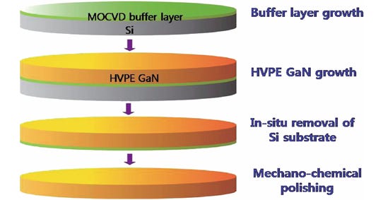
Schematic process steps for fabricating free-standing GaN-on-Si substrate using in-situ Si etching. Source
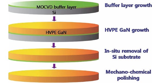
GaN vs SOI: SOI was about isolation (cleaning up silicon’s parasitic losses so low-power and signal-level chips run efficiently), GaN is about power: moving watts efficiently at speed. In an RF chain the two are complementary. SOI does the switching and control, GaN is the power amplifier.
Application: Power side (GaN-on-silicon): phone and laptop fast chargers, 48V AI-datacenter supplies, consumer and industrial power. RF side (GaN-on-silicon-carbide): 5G base stations, military radar, satellite links, defence.
Nature of business:
GaN-on-silicon power is a crowded scale-and-cost race, not a monopoly.
GaN-on-silicon-carbide RF is a concentrated oligopoly of a few specialists, now pulled more by defence and radar than by soft 5G telecom.
The higher-value bulk GaN corner (native crystal for vertical power devices) is an estimated 85%-plus Japanese oligopoly and gets interesting if vertical GaN scales.
Names to watch:
On-silicon: Navitas (NVTS), Innoscience (2577.HK) the Chinese IDM, Infineon (IFX.DE), STMicro (STM) and epi from IQE (IQE.L). fragmented
Bulk: Sumitomo Electric (5802.T), Mitsubishi Chemical (4188.T), Sciocs. Leader: Sumitomo Electric
On-SiC: Qorvo (QRVO), MACOM (MTSI), NXP (NXPI) and Sumitomo Electric (5802.T). Leader: Qorvo/MACOM
Indium phosphide, InP: the AI-optics dark horse
Problem it solves: silicon cannot make light (an indirect bandgap, if you want the term), so it will not emit a usable laser or detect light at speed. As AI datacenters move data as light (Photonics), that is a hard wall, and InP is the material that clears it, emitting and detecting light at very high speed.
Application: the lasers and photodetectors inside 800G and 1.6T optical modules are built on InP, so as hyperscalers push to those speeds, substrate demand follows. Also telecom long-haul, high-speed RF, sensing and LiDAR, and photonic integrated circuits.
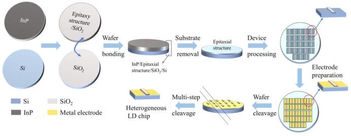
Nature of business: the purest listed expression of AI optics at the material level, small market today, real pull. The other name, alongside Soitec, that I most want to deep-dive. The pure-play carries central China exposure, a question for that deep dive.
Names to watch: Sumitomo Electric (5802.T) the anchor, Coherent (COHR) the integrated device-and-substrate play, AXT (AXTI) the US-listed pure-play (via a China subsidiary it is separately floating). Leader: Sumitomo Electric.
Honorable mentions: sapphire and the rest
Sapphire solves a narrow problem: you cannot grow an efficient blue LED on silicon (it absorbs the light and the lattices mismatch), so you need a transparent, insulating, lattice-friendly base. It doubles as scratch-proof cover glass on lenses and watch faces. Mature market, fragmented across mostly private names like Monocrystal, Rubicon and CoorsTek. Engineered and reclaimed silicon get a nod too. Named for completeness, not weighting.
One more substrate, and it is not a wafer
Everything above was the front-end substrate, the wafer the transistor is built on. The back-end substrate is where we finish.
Once cut from the wafer, the die cannot be soldered straight onto a board. It first mounts onto a package substrate, a dense multi-layer carrier.
The premium end (CPU/GPU substrates) is a tight group: Japan’s Ibiden (4062.T) and Shinko Electric (6967.T), Taiwan’s Unimicron (3037.TW) and Nan Ya PCB (8046.TW), Austria’s AT&S (ATS.VI), Korea’s Samsung Electro-Mechanics (009150.KS).
But the name nobody expects: the insulating film at the heart of virtually every high-end substrate is ABF, Ajinomoto Build-up Film, made by Ajinomoto (2802.T), the MSG-and-seasoning company. A food business with a near-monopoly on a material computing depends on.
This layer is being disrupted by glass, a story I have already told. This material pivot introduces a new group of supply chain beneficiaries: established glass materials giants (Corning, SKC/Absolics, SCHOTT) and Tier-1 display manufacturers (such as BOE Technology) pivoting legacy LCD glass-processing lines into advanced semiconductor packaging units.

Packaging substrate is a different industry that deserves its own map. Consider this an entree
Vote whether you would love the second part covering back end substrates too.
Conclusion
I am not telling you to buy a basket of wafer stocks, only where to look. The map sorts into three buckets, the “secure the base while you aim for the moon” logic.
Compounders (the base): Shin-Etsu (4063.T) and Sumitomo Electric (5802.T). Quality exposure to structural demand.
Cyclical oligopolists (the middle): SUMCO (3436.T), Siltronic (WAF.DE), GlobalWafers (6488.TWO), STMicro (STM), Infineon (IFX.DE). So far cyclical but can become structurally sound depending on AI capex.
Monopoly and moonshot single-bets (the small slice): Soitec (SOI.PA), AXT (AXTI), Navitas (NVTS), IQE (IQE.L), and the eyes-open Chinese plays SICC (688234.SH) and Innoscience (2577.HK).
I would like to conclude this post by saying that even thought I find a lot of interesting monopolies like IQE, SOI (holding), AXTI, one name has been on my watchlist for long: STMicro. Along with SOI, I think it is one of the names to own in this theme. They also have exposure to other business verticals.
But that’s a discussion for another day. Hope you enjoyed this post.
We do have a small favor to ask…
If you got value out of this article, we would really appreciate if you can spread the word amongst your friends, family or social media. We see it as a huge token of recognition from you. Thanks a lot for your time.
Any questions about this post or other things regarding stock market? Questions about some of our holdings? Let us hear them in the comments!
Please do restack, share and comment as a show of your approval (or disapproval) of the content
Glossary
Parasitic capacitance: A capacitor is just two conductors with an insulator between them. It stores charge, and it takes time and energy to charge and discharge. Each transistor sits directly on the conductive wafer, an unwanted capacitor forms between the two. Every time the transistor flips between on and off, it has to charge or drain that unwanted capacitor first. That takes a moment and burns a little power. Multiply across billions of transistors switching billions of times a second and it drags down speed and wastes energy.
Epitaxy (epi): an ultra-pure crystal film grown one atomic layer at a time on top of a finished wafer, carrying the active device while the bulk wafer underneath provides support.
Buried oxide (BOX): the thin glass (silicon dioxide) insulating layer sandwiched inside an SOI wafer, sitting under the thin working silicon and above the thick support silicon.
Latch-up: a failure mode in silicon logic where an unintended current path switches on and can destroy the chip; epi layers help suppress it.
Indirect bandgap: the property of silicon’s crystal structure that stops it emitting usable light, which is why light-emitting jobs need compound materials like indium phosphide.
Great read!
yes ,may soitec be better